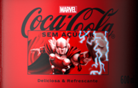
Products


Products

Researchers from KIT have developed novel X-ray detectors based on inkjet-printed perovskite semiconductors using a clever folding technology.


Products

OLED microdisplays have so far been developed predominantly on 200mm wafers. These conventional CMOS technologies and the associated backplane design have limited the number and size of pixels until now. At the Fraunhofer Institute for Organic Electronics, Electron Beam and Plasma Technology FEP (Dresden, Germany), OLED microdisplays have been realised for the first time in a 28-nanometre backplane technology on 300mm wafers within the "Backplane" project funded by the Saxon State Ministry of Economics, Labour and Transport (SMWA).


Products

PulseForge, Inc. (Austin, Texas) has announced the launch of its latest product, the PD 300 SA semi-automated photonic debonding tool. Designed to enable semiconductor advanced packaging for R&D and low-volume customers, this cutting-edge tool utilises the company’s patented photonic debonding process. This process leverages high-intensity pulses of light in conjunction with their proprietary, reusable, light-absorbing layer carriers to debond temporarily bonded materials for wafer thinning, hybrid bonding, and micro-LED transfer.